- Elon Musk announced Terafab on March 21, 2026, a $20-25 billion chip manufacturing facility to be built at the GigaTexas campus in Austin, Texas
- The facility targets one terawatt of annual AI compute capacity and 100,000 wafer starts per month initially, scaling to one million
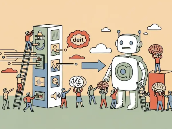
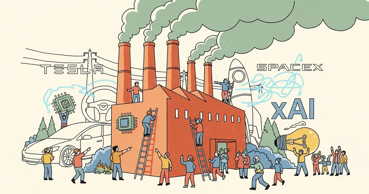
- Terafab is a joint venture between Tesla, xAI, and SpaceX, consolidating chip design, lithography, fabrication, memory production, and packaging under one roof
- Small-batch production of Tesla’s AI5 chip is anticipated in 2026, with volume production targeted for 2027
What Happened
Elon Musk announced Terafab on March 21, 2026, a semiconductor manufacturing facility that he described as the largest chip plant ever conceived. The factory will be built on the North Campus of GigaTexas in Austin, in a building planned to dwarf Tesla’s existing facility, which is already one of the largest structures in the world. Terafab is a joint venture between Tesla, xAI, and SpaceX, designed to consolidate every stage of semiconductor production under one roof. Tom’s Hardware reported on the formal launch during a livestream on X.
Why It Matters
Terafab represents a vertical integration play with no precedent in the semiconductor industry. By manufacturing its own chips, Musk aims to reduce his three companies’ dependence on external semiconductor suppliers, particularly TSMC and Samsung, for the custom silicon that powers Tesla’s autonomous driving systems, SpaceX’s satellite communications, and xAI’s Grok model training infrastructure.
The facility targets 2-nanometer process technology, placing it at the leading edge of semiconductor manufacturing. That capability is currently limited to TSMC, Samsung, and Intel’s foundry operations. Building a greenfield 2nm fab from scratch is among the most capital-intensive and technically challenging industrial projects possible. Intel’s own 2nm efforts have required over $100 billion in total investment across multiple facilities.
Technical Details
Terafab’s production targets are extraordinary by industry standards. The facility aims for one terawatt of annual AI compute capacity, with an initial target of 100,000 wafer starts per month scaling to one million. Annual output is projected at 100 to 200 billion custom AI and memory chips. For context, one terawatt of computing capacity would theoretically power over 1.4 million Nvidia H100-equivalent processors running continuously, a scale that exceeds any single company’s current compute deployment.
The facility will produce two distinct processor categories: terrestrial inference chips for Earth-based applications and space-hardened processors for aerospace operations. Tesla’s AI5 chip, the fifth-generation autonomous driving processor, will be among the first products manufactured at Terafab. The factory consolidates chip design, lithography, fabrication, memory production, advanced packaging, and testing, an end-to-end approach that mirrors Apple’s vertical integration strategy with its M-series silicon but at a significantly larger scale.
Who’s Affected
The joint venture structure across Tesla, xAI, and SpaceX creates governance questions that Musk’s companies have navigated before. Tesla shareholders may question whether the factory’s output will be allocated fairly across the three entities, particularly if xAI’s training compute demands compete with Tesla’s need for autonomous driving chips. The $20-25 billion investment will need to be funded across the three companies, though the specific capital allocation among Tesla, xAI, and SpaceX has not been disclosed. Board-level conflicts of interest are a recurring concern given Musk’s controlling role across all three entities.
For the broader semiconductor industry, Terafab signals that major AI consumers are increasingly willing to build their own chip supply rather than remain dependent on foundry partners. This follows similar moves by Google with its TPU line and Amazon with its Trainium and Graviton chips, though neither has attempted in-house fabrication at this scale.
What’s Next
Small-batch production of Tesla’s AI5 chip is anticipated later in 2026, with volume production targeted for 2027. The timeline is aggressive given that semiconductor fab construction typically takes three to five years from groundbreaking to volume production. Whether Musk’s $20-25 billion budget is sufficient for a cutting-edge 2nm facility remains an open question. Intel’s comparable efforts have required over $100 billion across multiple sites.
The project also faces workforce challenges. Advanced semiconductor manufacturing requires thousands of specialized engineers and technicians, a talent pool that TSMC, Samsung, and Intel are already competing fiercely to recruit. Musk has not detailed how Terafab will attract this expertise to Austin, or whether the facility will partner with an established foundry operator for process development. The long-term goal of one million wafer starts per month would require sustained capital expenditure well beyond the initial investment and a manufacturing workforce that does not currently exist outside of established Asian fabs.