- A former Google TPU and NVIDIA engineer published a comprehensive framework covering every layer of custom AI chip design, from workload analysis to compiler implementation.
- The document addresses a critical knowledge gap by showing how hardware architecture decisions and software stack choices constrain each other across the full design space.
- With dozens of AI chip startups competing against NVIDIA, the paper provides a practical checklist of integration challenges that teams often discover too late in development.
What Happened
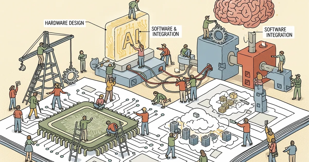
A detailed technical document shared on r/MachineLearning on March 22 lays out a complete framework for designing AI chip software and hardware from scratch. The author, who previously worked on Google’s Tensor Processing Units and NVIDIA GPU performance characterization, maps the entire design space from workload analysis through architecture selection to compiler and runtime implementation.
The paper connects layers that are typically discussed in isolation, showing how decisions at the algorithm level constrain hardware design and vice versa. Individual components like attention mechanisms, quantization schemes, and memory hierarchies are well-documented separately, but their interactions across the stack are rarely treated in a unified framework. The document fills that gap by walking through how each layer’s design choices ripple up and down the stack.
Why It Matters
Dozens of AI chip startups are currently competing to build alternatives to NVIDIA’s GPUs. Most focus on narrow performance claims — faster attention computation, cheaper inference, lower power consumption — without addressing the full-stack integration challenges that determine whether a chip succeeds in production environments.
The document serves as both a technical reference and a cautionary guide. Building competitive AI silicon requires simultaneous optimization across algorithms, architecture, compilers, and runtime systems. Few teams have the cross-disciplinary expertise to execute across all of these layers, and the author’s experience at both major silicon vendors lends credibility to recommendations that might otherwise remain theoretical. As one commenter on the Reddit thread noted, “This is the document I wish existed when we started our chip project two years ago.”
Technical Details
Key technical contributions include analysis of memory bandwidth bottlenecks across different AI workloads, comparison of dataflow architectures for transformer inference versus training, and guidelines for mapping operator graphs to custom silicon. The paper also covers practical considerations for compiler design targeting non-standard architectures.
The author draws on experience with both Google’s and NVIDIA’s approaches to illustrate specific tradeoffs between programmability and efficiency. For instance, Google’s XLA and MLIR compilation chains demonstrate how specialized chips often require more complex compilation pipelines, while NVIDIA’s CUDA ecosystem shows the advantages of broader programmability at the cost of silicon efficiency.
According to industry data, as of 2026, 50 percent of high-performance computing chip design uses multi-die approaches, with expectations for another 20 to 25 percent growth. The market has also shifted its primary focus from training workloads in data centers toward inference optimization. The paper addresses both use cases, noting that training and inference impose fundamentally different demands on memory subsystems, arithmetic precision, and inter-chip communication — tradeoffs that most chip startups underestimate during initial architecture exploration.
Who’s Affected
The paper is directly relevant to AI chip startups and their engineering teams who face the challenge of building complete software stacks alongside novel hardware. It also matters for AI infrastructure teams at cloud providers evaluating custom silicon options, and for ML engineers who need to understand why certain hardware platforms perform differently than benchmark numbers suggest.
Venture investors funding AI hardware companies may find the document useful as a technical due diligence checklist, since it highlights integration challenges that are easy to overlook when evaluating early-stage chip designs based on simulation results alone. Companies like Cerebras, Groq, and SambaNova have each taken different positions on the programmability-efficiency spectrum the paper describes, and the framework helps contextualize those architectural bets.
What’s Next
The document is publicly available for download, though the author has not indicated plans to expand it into a formal academic publication. Community discussion on Reddit has focused on specific sections covering compiler design and memory hierarchy optimization, with several engineers from chip startups contributing additional context on real-world implementation challenges.
The paper does not cover manufacturing, supply chain, or cost modeling considerations, which remain separate but equally significant barriers for new entrants in the AI chip market. It also does not address the emerging trend of model-chip co-design — where ML architectures are tailored to specific hardware during training — a topic that Meta recently explored in its MTIA 2i productionization paper.
Related Reading
- Apple Research Exposes Critical Gaps in Multimodal AI Safety
- Where Are All the AI Apps? Answer.AI Examines the Application Gap
- App Store New Submissions Jump 30% to 600,000 in 2025 as AI Coding Tools Scale
- Software Engineer Warns AI Code Generation Creates $10T Maintenance Crisis
- Zuckerberg Develops AI Agent to Handle CEO Duties at Meta