- Cognichip closed a $60 million Series A to scale its AI-driven semiconductor design platform, which compresses chip design timelines from months to weeks.
- The company directly challenges EDA incumbents Cadence Design Systems and Synopsys by automating key steps in the chip layout and verification process.
- The funding signals growing investor confidence in a recursive loop: AI systems designing the hardware that will run the next generation of AI.
- Major semiconductor firms and hyperscalers are already evaluating AI-assisted EDA tools as chip complexity outpaces human engineering capacity.
What Happened
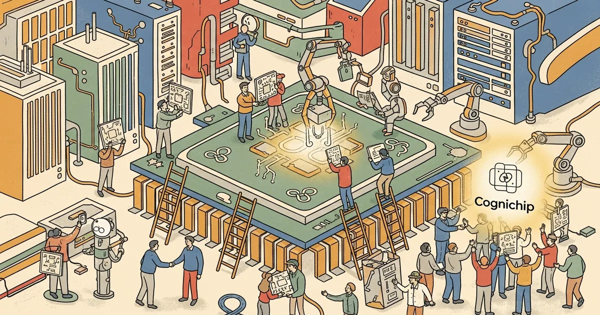
Cognichip, a startup focused on applying artificial intelligence to semiconductor design, closed a $60 million Series A funding round in early April 2026. The company’s platform uses machine learning models to automate portions of the electronic design automation (EDA) workflow — the complex, multi-stage process of turning a chip specification into a manufacturable layout.
Traditional EDA flows involve months of work by specialized engineers using tools from Cadence Design Systems and Synopsys, the two companies that collectively dominate the $15 billion EDA market. Cognichip’s pitch is that AI can handle critical bottlenecks in this process — including floor planning, placement, routing, and timing closure — at a fraction of the time and cost.
The round positions Cognichip to expand its engineering team and deepen integrations with foundry design rule decks, particularly at advanced nodes (5nm and below) where design complexity has grown exponentially.
Why It Matters
The semiconductor industry is caught in a capacity crunch. As chips grow more complex — modern AI accelerators contain tens of billions of transistors — the engineering hours required to design them have ballooned. A single advanced chip design can cost over $500 million and take two to three years from specification to tape-out. The pool of engineers qualified to do this work is not growing at the same rate.
AI-assisted chip design addresses this bottleneck directly. Google’s DeepMind published research in 2021 showing that reinforcement learning could produce chip floor plans competitive with human experts in hours rather than weeks. Since then, both Cadence and Synopsys have invested heavily in adding AI features to their own tools — Synopsys with its DSO.ai platform and Cadence with Cerebrus. But these are bolt-on enhancements to legacy codebases built over decades.
Cognichip represents a bet that a purpose-built, AI-native approach can outperform the incumbents. If it works, the implications extend beyond efficiency. This is AI designing the silicon that runs AI — a recursive loop that could accelerate hardware progress independently of Moore’s Law scaling.
Technical Details
Cognichip’s platform reportedly uses a combination of graph neural networks and reinforcement learning to optimize chip layouts. The system ingests design rule files from foundries (the manufacturing constraints that dictate how transistors and interconnects can be arranged) and learns to produce layouts that meet timing, power, and area targets simultaneously.
Three technical claims distinguish the platform from incumbent tools. First, Cognichip says its placement engine can explore 10x more design configurations than traditional tools in the same compute budget, thanks to learned heuristics rather than rule-based search. Second, the platform performs timing closure — the notoriously iterative process of ensuring all signals arrive at the right place at the right time — with fewer iterations. Third, the company claims its routing algorithms reduce wire length by 8-12% on benchmark designs, which translates directly to lower power consumption.
These are engineering claims that will need validation at production scale. The EDA industry has seen bold startup claims before; the question is whether Cognichip can handle the full complexity of real-world tapeouts at advanced nodes, where corner cases multiply and manufacturing tolerances shrink to atomic scales.
Who’s Affected
The most immediate impact falls on Cadence and Synopsys, which together hold roughly 70% of the EDA tools market. Both companies trade at premium valuations partly because of the deep moats created by decades of accumulated design rule knowledge and customer lock-in. An AI-native competitor that can match their output quality would erode those moats.
Chip design teams at hyperscalers — Google, Amazon, Microsoft, and Meta all design custom silicon now — stand to benefit from faster design cycles. Startups building AI accelerators, such as Cerebras, Groq, and SambaNova, could also use AI-driven EDA to iterate on architectures more quickly without maintaining massive internal design teams.
Foundries like TSMC and Samsung may need to adapt their design kit ecosystems to accommodate AI-native tools, which could require new interfaces and validation workflows.
What’s Next
Cognichip will need to demonstrate production tapeouts — actual chips manufactured using its AI-generated layouts — to convert skeptics. The EDA industry runs on trust built over decades of proven silicon, and no amount of benchmark performance will substitute for working chips in customer hands.
The broader trend is clear: AI-assisted chip design is moving from research curiosity to commercial necessity. Cadence and Synopsys are not standing still, and both have the customer relationships and design rule libraries to defend their positions. The next 18 months will determine whether Cognichip can break into production workflows or whether the incumbents absorb AI capabilities fast enough to neutralize the threat.
The recursive dynamic — AI improving the hardware that makes AI faster — adds a strategic dimension that extends well beyond the EDA market. Investors and national security planners are watching closely.